January
29, 2017
(modified on October 5, 2017)
My Book
Chapter in
"Chemical Vapor Deposition (CVD): Types, Uses and Selected
Research"
Have you ever learned junction
formation process as a key technology in semiconductor devices?
This field is full of science of materials and phenomena
which are hardly seen by human eyes. How do we see the real face
and behavior of materials?
I wrote a chapter on semiconductor
process in a specialized book as follows. The content is related to various fields of material
science, engineering and physics of nanoelectronic devices.
- - - - - - - -
In the city of
Sapporo at northern land of Japan, there was a high school student
who wanted to study semiconductor. When connecting several ICs
(integrated circuits) like a black centipede, a computer can be
made. The high school student was interested in such a thing.
"What kind of structure does the IC have?"
"How is the IC fabricated?"
"What kind of technology is missing to improve performance?"
He wanted to know concretely. However, the Internet has not yet
been popular at the time. When he was looking for specialized
books at book stores, he could not find easy ones to be understood
by very ordinary high school students. He thought he had no idea
who can kindly guide him about it.
Though he just started to study programming, his interest in it
had gone somewhere. He decided to go to university to study
unknown world of semiconductors in the ICs.
It should be noted that it was easy for him to decide it. Because
his head had got filled by a thought "I just want to learn it!",
there was no room for other thoughts to compete. Besides that, his
parents and family did not complain anything about his dicision
and they supported him gently. It was great help for him.
After that, what happened to the high school student?
He has graduated a university at the city
of Sendai and also been working as the
university teacher for more than 20 years. Of course, he has been
studying semiconductors.
His dream has come true.
Interestingly, Sendai was not the course he had originally
planned. It was an unfamiliar place for him and he did not know
almost anything about on-going history of the university at
Sendai.
Moreover, very surprisingly, the university was filled with a
plenty of conditions and timing necessary for his studying
semiconductor. He could never regard it as just a rare
coincidence. He believed it was a destiny which had been prepared
previously.
In this way, the high school student has become a researcher of
semiconductor. For young students visiting to the laboratory, he
is teaching how to proceed researches and how to write academic
papers. He is also giving lectures on paths up to achievements and
useful ideas in research.
That is me.
- - - - - - - -
You will find a few key points of state-of-the-art semiconductor device fabrication and a reason why we study on plasma CVD for the devices. Additionally, you will find a scene of creation of new material in the field of material science.Although it is specialized for
engineers and material scientists, I would appreciate if many
people could read the chapter to know my activity and prospects in
research as well as the way of my thinking.
Chapter
4 :
"Low-Energy Plasma CVD for
Epitaxy and In-Situ Doping of Group-IV Semiconductors in
Nanoelectronics",
Masao Sakuraba, Hisanao
Akima and Shigeo Sato,
Laboratory for Nanoelectronics
and Spintronics, Research Institute of Electrical
Communication, Tohoku University
pp.61-115
>> How to read my chapter on FREE PDF <<
|
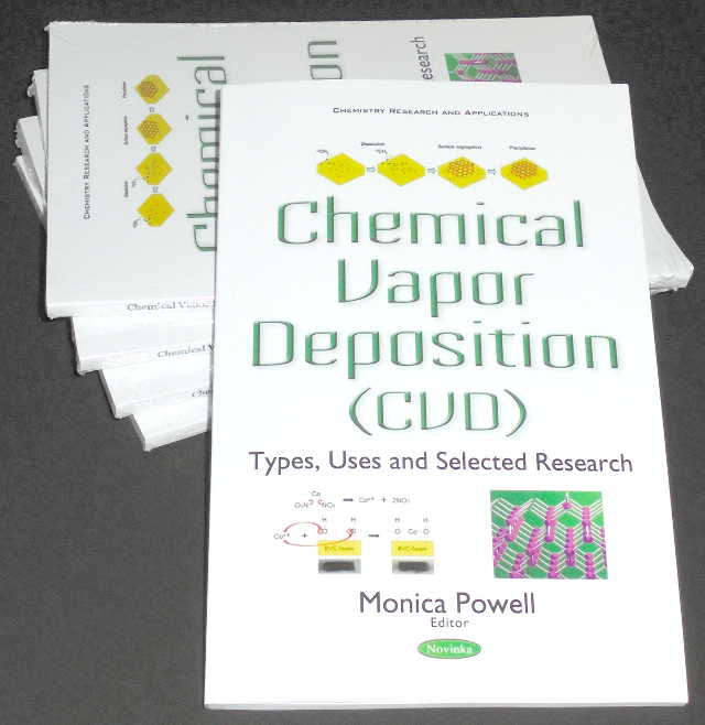
Book Title :
"Chemical Vapor Deposition
(CVD): Types, Uses and Selected Research"
(Edited by Monica Powell, Nova Science Publishers, Inc.,
Feb. 14, 2017).
Links to Publisher |
||
|
||
4.1 Introduction
4.2 Epitaxy as a Technology Driver in Si LSI
4.3 Surface Orientation and Hydrogen Termination of Silicon Surface for Low-Temperature Epitaxy
4.4 Low-Energy ECR Plasma CVD Processing
4.5 Epitaxy of Silicon and Germanium
4.6 Epitaxy of Silicon-Germanium Alloy
4.7 Epitaxy of Silicon-Carbon Alloy
4.8 In-Situ Doping of Boron in Silicon and Germanium Epitaxy
4.9 Atomic-Layer Doping of Boron in Silicon Epitaxy
4.10 Low-Stress Silicon Nitride Filim Formation under Low-Energy Nitrogen Plasma Irradiation
4.11 Smart Plasma Process for Semiconductor Device Fabrication
4.12 Challenge of Crystal Structure Transformation in Silicon Nano Sheet by Plasma-Induced Reconstruction
4.13 Conclusions and Future Prospects
>> How to
read my chapter on FREE PDF <<
P.68 L4-13 "For new horizon in the integration of state-of-the-art semiconductor devices, e.g., Esaki-tunnel FET and resonant-tunneling diodes/transistors, control of subnanometer-order (atomic-order) abrupt intefaces will be necessary in the p-n junctions and heterojunctions, because quantum-tunneling and confinement phenomena are sensitively determined by nanometer-order tunnelling distance. In order to enhance and control the quantum phenomena, ultimately-localized two-dimensional (2D) doping and energy-band modulation using the abrupt-interface heterostructures will become important increasingly. In such a trend, lower-temperature process for epitaxy and in-situ doping is apparently necessary and must be pursued."
P.104 L10-21 "Si LSI has become indispensable not only for personal-level and global-scale information and communication technology but also for many kinds of small or large electronically-controlled systems. Vast fields of materials science and engineering have been contributing to the technology. Therefore, it is sure that technology provides convenience to people, however from perspective on humanity e.g., dignity of life, we had better to remind ourselves that, in order to achieve one person's convenience, another person's life should not be sacrificed. Thereon, technology should be used not for killing someone but for providing peace for all of human beings on the Earth. It seems natural that such a mind always exists behind development of technology. Even if we have freedom to choose any purpose to use technology or we have no intention to choose, we are responsible for the choice eternally."
>> How to read my chapter on FREE PDF <<
|
Book Title :
"Chemical Vapor Deposition
(CVD): Types, Uses and Selected Research"
(Edited by Monica Powell, Nova Science Publishers, Inc.,
Feb. 14, 2017).
Links to Publisher |
||
|
||
>> How to read my chapter on FREE PDF <<
Return to Top Page