ペンタグラフェン(ペンタシリセン)の模型試作
Penta-Graphene (Penta-Silicene) Model
Aug. 22, 2016 Masao Sakuraba
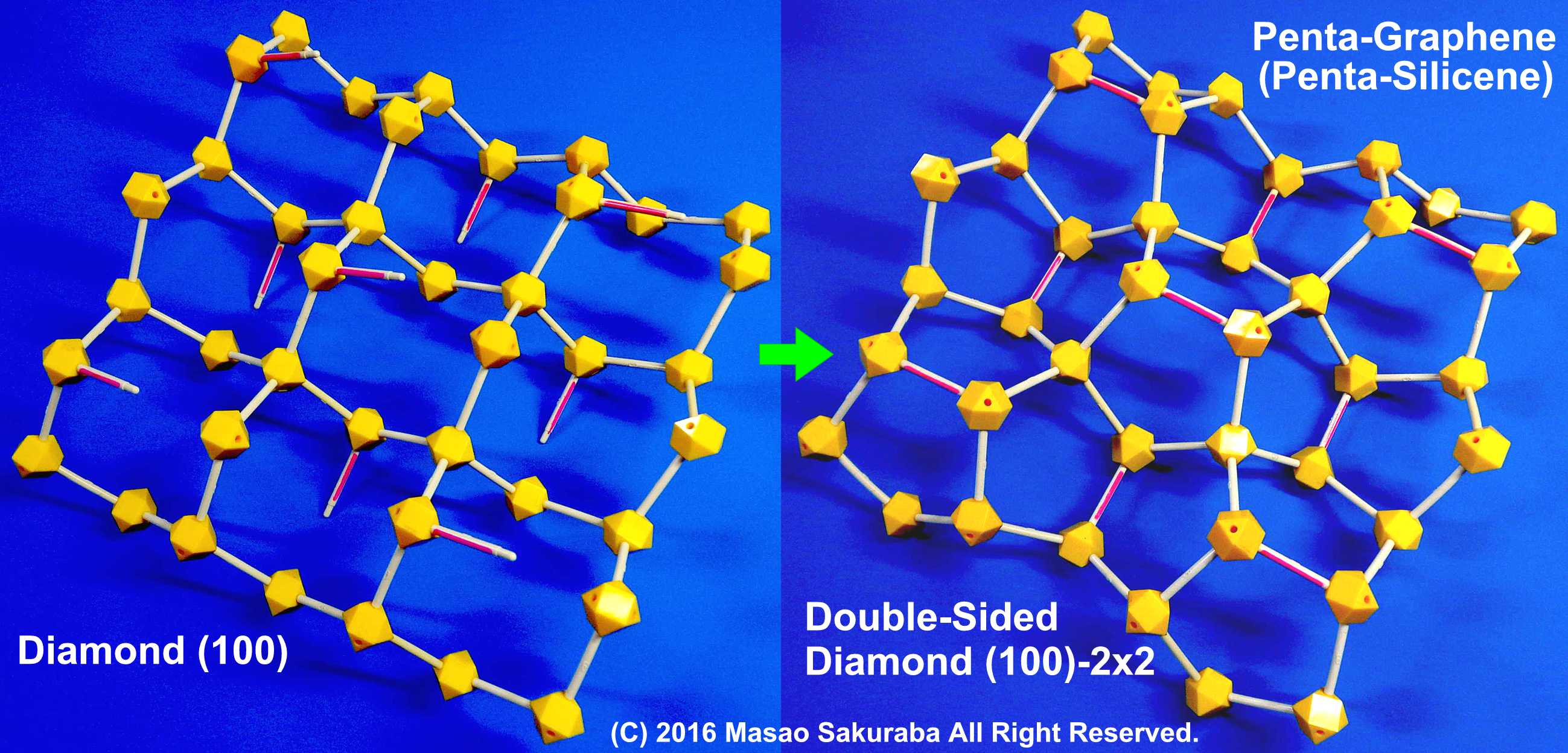
川添良幸先生に教えて頂いたペンタグラフェンを(100)面から作る手順についてアイデアが浮かんできましたので、以下に原子模型を使って説明してみます。(【追記】 詳細を著書[Ref. 3]にまとめました。)
- (手順1)ダイヤモンド(100)面を3原子層分だけ作る。(両面ともdiamond (100)-1x1)
- (手順2)ダングリングボンド(ピンク色)で原子を引き寄せてダイマーを作る。(両面ともdiamond (100)-2x2)
炭素をシリコンやゲルマニウムに置き換えれば、ペンタシリセンやペンタジャーマネンと呼ばれます。
Concerning a penta-graphene (Prof. Yoshiyuki Kawamata taught the model to me), I have come up with an idea of how to make it. I try to show the idea by using the atomic model. (P.S. Details have been summarized in my book chapter [Ref. 3].)
- (1) Make a (100) diamond of 3 atomic layers. (Double-sided diamond (100)-1x1)
- (2) Dimerize for pink dangling bonds on both sides. (Double-sided diamond (100)-2x2)
If carbon is replaced by silicon or germanium, it is called "penta-silicene" and "penta-germanene", respectively.
実際に模型を組み立ててみると、中間層原子の周期的ねじれによって、正四面体の自然な結合角度が保たれ、ダイマー形成ストレスは非常に小さいことがわかりました。
When I made the model, I could easily feel that stress for dimerization is quite small under keeping natural bonding angle of tetrahedron thanks to periodic twisting of mid-layer atoms.
上記の手順のように理想的なエピタキシャル成長を実現させ、選択的に下地を溶かすことができれば、自然にペンタグラフェンができそうな気がしてきます。
If such an ideal 3 atomic-layer film can be epitaxially grown and substrate material can be removed selectively, it might come true naturally.
実現への鍵は、ヘテロエピタキシャル成長やサスペンド構造形成の技術開発の進展でしょう。
Key technolgy is a method for heteroepitaxial growth and suspended membrane structructure formation.
|
|
References
| 1. | 東北大学プレスリリース、2015年4月21日 15:00、 ”五角形のグラフェンの発見-夢の新素材として期待-”. http://www.tohoku.ac.jp/japanese/2015/04/press20150421-02.html |
| 2. | "Penta-graphene: A new carbon allotrope" Shunhong Zhang, Jian Zhou, Qian Wang, Xiaoshuang Chen, Yoshiyuki Kawazoe, and Puru Jena, Proc. Natl. Acad. Sci. USA, Vol.112, (2015), pp.2372–2377. doi: 10.1073/pnas.1416591112 http://www.pnas.org/content/112/8/2372 |
| 3. |
“Low-Energy Plasma CVD for Epitaxy
and In-Situ Doping of Group-IV Semiconductors in Nanoelectronics”,
M. Sakuraba, H. Akima and S. Sato, Chapter 4 in “Chemical Vapor Deposition (CVD): Types, Uses and Selected Research”, ed. M. Powell, (Nova Science Publishers, Inc., New York, Mar, 2017), [Book] ISBN 978-1-53610-893-4, pp.61-115; [eBook] ISBN 978-1-53610-908-5. http://www5a.biglobe.ne.jp/~tenrou/books/index.htm |